
Thick Film Hybrid IC
Ordering number : EN4867A
O1895HA (OT)/N0794TH (OT) No. 4867-1/10
SANYO Electric Co.,Ltd. Semiconductor Bussiness Headquarters
TOKYO OFFICE Tokyo Bldg., 1-10, 1 Chome, Ueno, Taito-ku, TOKYO, 110-8534 JAPAN
Unipolar Fixed-Current Chopper-Type
4-Phase Stepping Motor Driver
STK6712BMK4
Overview
The STK6712BMK4 is a unipolar fixed-current chopper-
type 4-phase stepping motor driver hybrid IC (HIC) which
uses a MOSFET power device. The excitation sequence
signal is active low.
Applications
∑ Serial printer, line printer, and laser beam printer (LBP)
paper feed and carriage motor drivers
∑ PPC scanner and LBP paper feed drivers
∑ XY plotter pen drivers
∑ Industrial robot applications, etc.
Features
∑ This IC has the features of the STK6712BMK3, plus a
simultaneous input prevention circuit that protects the
IC from any malfunction of the excitation signal.
∑ Self-excitation design means chopping frequency is
determined by motor L and R. Supports chopping at
20 kHz or higher.
∑ Very low number of external components required.
∑ Wide operating supply voltage range (V
CC
1 = 18 to
42V)
∑ Excitation sequence signal is active low, and is TTL
level for direct interfacing to the microcomputer and
gate array.
∑ The unipolar design enables use as a driver for hybrid,
PW, or VR type stepping motors.
∑ Supports W1-2 phase operation, with a dual Vref pin.
Package Dimensions
unit: mm
4129
[STK6712BMK4]

Specifications
Maximum Ratings
at Ta = 25∞C
Allowable Operating Ranges
at Ta = 25∞C
Junction Thermal Resistance
Electrical Characteristics
at Tc = 25∞C, V
CC
1 = 36 V, V
CC
2 = 5 V
Note: With constant voltage power supply.
Internal Equivalent Circuit
No. 4867-2/10
STK6712BMK4
Parameter
Symbol
Conditions
Ratings
Unit
Maximum supply voltage 1
V
CC
1 max
No input signal
52
V
Maximum supply voltage 2
V
CC
2 max
No input signal
7
V
Maximum phase current
I
OH
max
per phase, R/L = 5
, 10 mH, 0.5 s 1 pulse, V
CC
input
2.5
A
Substrate temperature
Tc max
105
∞C
Junction temperature
Tj max
150
∞C
Storage temperature
Tstg
≠40 to +125
∞C
Repeated avalanche resistance
Ear max
38
mJ
Parameter
Symbol
Conditions
Ratings
Unit
Supply voltage 1
V
CC
1
With input signal
18 to 42
V
Supply voltage 2
V
CC
2
With input signal
4.75 to 5.25
V
Phase driver voltage resistance
V
DSS
(min) 120
V
Phase current
I
OH
max
Duty 50%
(max) 1.7
A
Parameter
Symbol
Conditions
Ratings
Unit
Power FET
j-c
13.5
∞C/W
Parameter
Symbol
Conditions
min
typ
max
Unit
Output saturation voltage
V
ST
R
L
= 23
, V
IN
= 0.8 V
1.1
1.5
V
Output current (average)
Io ave
R/L = 3.5
/3.8 mH, V
IN
= 0.8 V per phase
0.45
0.50
0.55
A
Pin current dissipation (average)
I
CC
2
Load, R = 3.5
, L = 3.8 mH, V
IN
= 0.8 V per phase
15
25
mA
FET diode voltage
Vdf
Idf = 1.0 A
1.2
1.8
V
TTL input ON voltage
V
IH
Input voltage when F1, 2, 3, 4 ON
2.0
V
TTL input OFF voltage
V
IL
Input voltage when F1, 2, 3, 4 OFF
0.8
V
Switching time
t
ON
R
L
= 24
, V
IN
= 0.8 V
100
ns
t
OFF
R
L
= 24
, V
IN
= 0.8 V
0.2
µs

Sample Application Circuit
Note: For reference, when I
OH
1.1 A, R
O
1 = 6.8 k
and R
O
2 = 390
.
I
OH
= K
◊
◊
V
CC
2/R
7
K
1.3
R7 = R8
0.33
± 3%
To reduce noise during motor hold, it is possible to mount C
O
1
0.01 µF and C
O
2 = 100-200 pF. Normally these are
not required.
STK6712BMK4 Circuit Operation
Fig. 1 STK6712BMK4 Internal Equivalent Circuit
R
O
2
R
O
1 + R
O
2
No. 4867-3/10
STK6712BMK4
Output current waveform when phases are held (locked)
Measure output current values in this state.

The operation for a 4-phase dual-excitation example is described below.
The STK6712BMK4 equivalent circuit is given in Fig. 1. The circuit consists of the phase drivers, the comparator, the
PWM excitation select and the current detect resistance. In Fig. 1 ¯A is input with low, and ¯A with high. When Q1
goes on, the +pin of IC1 (comparator) goes low, making IC1 output
low also. A winding current i
ON
through Q1
increases as:
i
ON
=
(1 ≠ e
) ........................................................................................................... (1)
L: motor winding inductance
R: Sum of winding resistance and current detect resistance
For this reason, pin voltage V
R7
at source resistor R7 increases, and when the V
RO
2 voltages of pin 8 and R
O
2 are equal
output A goes high, and Q1 turns off. The inverse voltage V
TP
is as:
V
TP
= Vref =
◊
V
CC
2.......................................................................................................... (2)
In general stepping motor coils use BIFALAR windings, so the energy stored in L1 is generated by L2, at which time the
current in L2 is i
OFF
. i
OFF
conduction continues until the charges of capacitors C1 and C2 on R3 and R4 pins (E
C
) equal
V
RO2
. When they are equal, output
inverts and becomes low. Motor winding current i
ON
again rises to V
RO2
level.
This motor current on/off (constant current chopping) is repeated. This waveform is illustrated on the next page.
STK6712BMK4 Basic Circuit
S
R
O
2
R
O
1 + R
O
2
≠
t
R
L
V
CC
1 ≠ V
SAT
R
S
No. 4867-4/10
STK6712BMK4

Waveform Timing Charts
Fig. 2
Control Logic Timing Chart
1. 2-phase excitation
No. 4867-5/10
STK6712BMK4
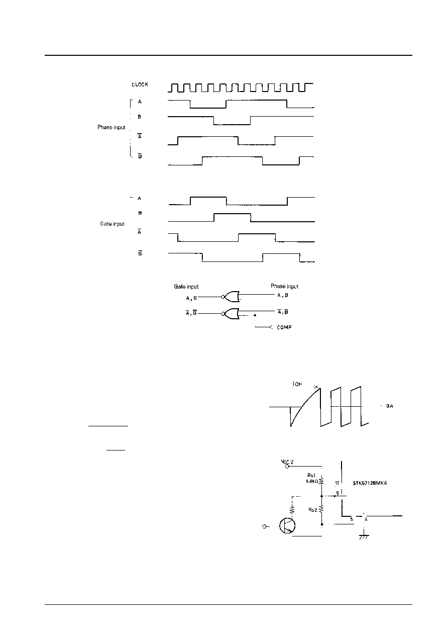
2. 1-2 phase excitation
STK6712BMK4 Excitation Circuit
Setting Output Current
The motor output current waveform is shown to the right.
Output current I
OH
can be set by the user by adjusting the
voltage of pin 9 (11).
The computation equation is indicated below.
Vref =
◊
V
CC
2...............................(3)
I
OH
K
◊
...............................................(4)
R
S
: Internal current detect resistance
(0.33 ± 3%)
K: 1.1 to 1.2 (correction for actual measurement)
Power down can be accomplished by reducing the synthetic
impedance by connecting a resistance in parallel to R
O
2.
The motor output current variation range can be set for the
range of:
I
OH
= 0.2 A to 1.7 A
but when set to I
OH
= 0.2 A or lower note that the HIC GND pattern will be one-point earth with respect to the power
supply. If earth is poor, there may be no motor current when I
OH
= 0.2 A. We recommend a motor inductance usage
range of L = 1 mH to 10 mH.
Vref
R
S
R
O
2
R
O
1 + R
O
2
No. 4867-6/10
STK6712BMK4
Fig. 3 Output Motor Current Waveform
Fig. 4 Vref Peripheral Circuit

Determining Chopping Frequency
The STK6713BMK4 uses constant current for self-excitation.
The I
OH
t
OFF
time is set to about 14 µs, and the t
ON
time can be expressed as:
L
V
CC
≠ ( I
OH
e
≠
V
CC
+ 0.88
(1 ≠ e
)) (R + 0.88)
t
ON
R + 0.88
In (
R
) ............................ (5)
V
CC
≠ (R + 0.88) I
OH
L:
Motor winding inductance
R:
Motor resistance
V
CC
: Motor supply voltage
I
OH
:
Output current
As a result, the chopping frequency is
F
=
(Hz) ................................................................................................ (6)
However, note that when the following conditions exist the value for F will change.
14
◊
10
≠6
In (
) = t
OFF
2 ............................................................................. (7)
t
OFF
t
OFF
1 + t
OFF
2 = 14
◊
10
-6
+ t
OFF
F =
(Hz)........................................................................................................ (8)
Because the STK6712BMK4 is self-exciting there will be minor variation in motor inductance during motor revolution.
Final design verification is required in an actual model.
Thermal Radiation Design
The HIC radiator plate size is dependent on the motor output current I
OH
(A), motor electrical characteristics, excitation
mode, and excitation input signal clock frequency fclock (Hz).
The thermal resistance for the radiator can be determined from the following expression.
c ≠ a =
(∞C/W).................................................................................................................. (9)
Tc max = HIC substrate temperature
(∞C)
Ta = set internal temperature
(∞C)
Pd = HIC internal mean power dissipation (W)
Tc max ≠ Ta
Pd
1
t
ON
+ 14
◊
10
≠6
+ t
OFF
2
V
CC
+ 0.88
I
OH
◊
R + V
CC
+ 0.88
≠L
R
1
t
ON
+ 14
◊
10
≠6
1
t
ON
+ t
OFF
≠
t
OFF
R
L
≠
t
OFF
R
L
No. 4867-7/10
STK6712BMK4

With a 2.00 mm aluminum radiation plate, the required area can be determined from Fig. 6. Note that substrate
temperature will vary widely with set internal air temperature, and therefore the rear side of the HIC (the aluminum plate
side) must always be kept below the maximum temperature of 105∞C.
HIC Internal Mean Power Dissipation Pd
The internal mean power dissipation of the STK6712BMK4 is primarily due to the current control device, the
regenerating current diode, the current detect resistance and the predriver circuit.
Loss in each excitation mode is:
2 phase excitation
Pd2
EX
(Vst + Vdf)
I
OH
t2 +
I
OH
(Vst
◊
t1 + Vdf
◊
t3)
..................................... (10)
1-2 phase excitation Pd1 ≠ 2
EX
(Vst + Vdf)
fclock +
fclock (Vst
◊
t1 + Vdf
◊
t3)
..................................... (11)
Vst:
R
ON
voltage drop + R7 (R8) output voltage
Vdf:
FET internal diode + R7 (R8) output voltage
fclock:Input clock (reference frequency before frequency divider)
t1, t2 and t3 are the time modes for the waveform indicated below.
t1: Time for winding current to rise to set current
t2: Time for constant current chopping region
t3: Time from end of phase input signal until inverse current regeneration is complete.
Fig. 7 Motor Output Current Waveform (model)
3I
OH
3
3I
OH
t2
8
fclock
2
fclock
2
No. 4867-8/10
STK6712BMK4
Fig. 5
Fig. 6
t1
In (1 ≠
◊
I
OH
) .............................................................................................. (12)
t3
In (
) ...................................................................................................... (13)
V
CC
: Motor supply voltage (V)
L :
Motor inductance (H)
R :
Motor internal resistance (
)
I
OH
: Motor output current peak (A)
The chopping frequency F and t2 for each excitation mode are:
2 phase excitation
F = fclock/2, t2 = (1/F) ≠ (t1 + t3).......................................................................... (14)
1-2 phase excitation F = 3fclock/8, t2 = (1/F) ≠ t1.................................................................................. (15)
fclock: 4-phase divider input oscillation frequency
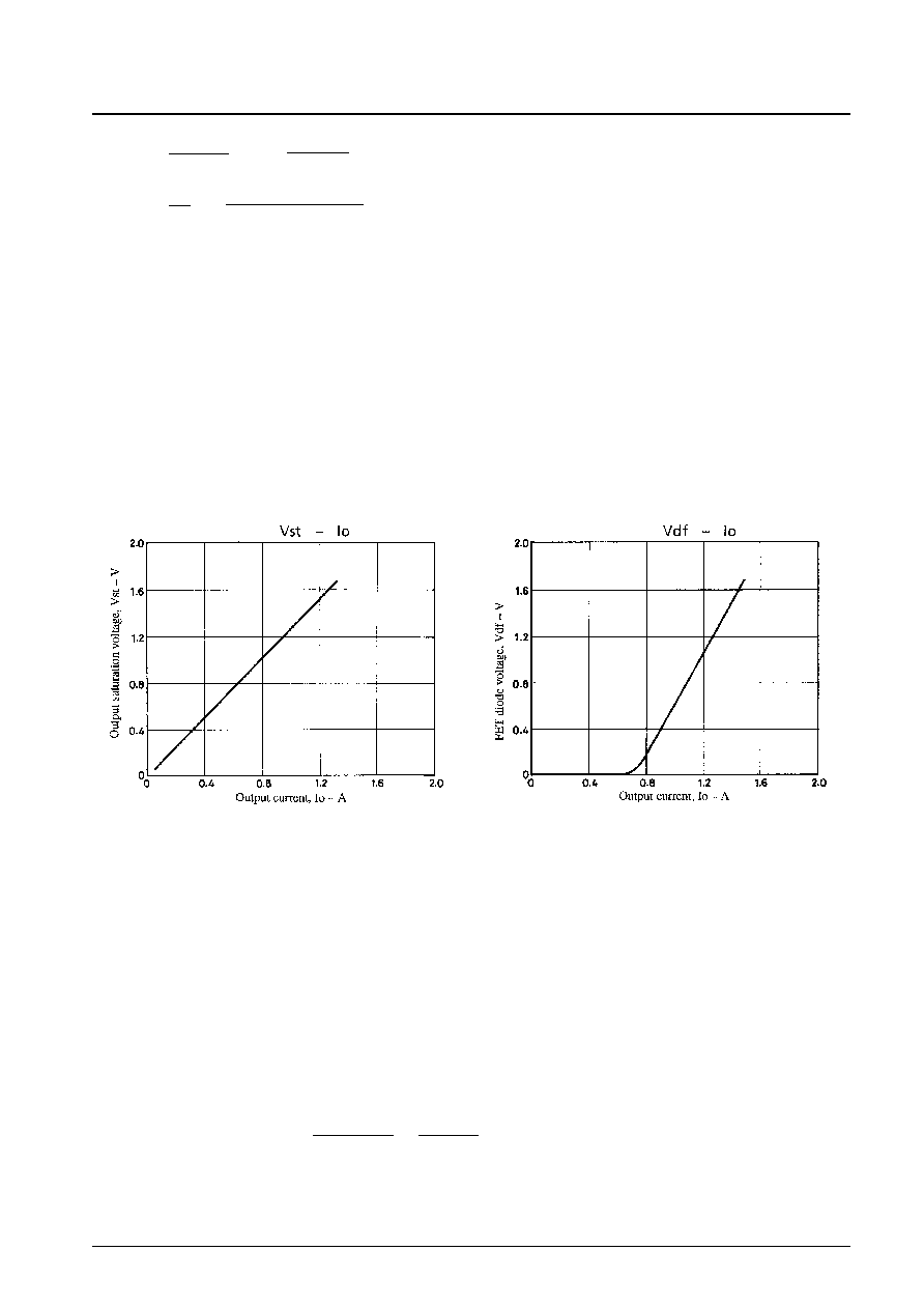
The characteristic diagrams (typ) for I
OH
and Vst, and I
OH
and Vdf are given in Figs. 8 and 9.
STK6712BMK4 No Thermal Radiation Range (example)
An example of STK6712BMK4 use in the no-fin state is indicated below.
Conditions:
∑ Motor supply voltage V
CC
1 = 30 V, stepping motor: Electrical characteristics 3.5 mH/¯, 3.5
/¯
∑ Excitation: 2-phase
∑ Input clock frequency 500 Hz = fclock
∑ HIC ambient temperature Ta = 25∞C, natural convection
∑ HIC rear substrate temperature Tc = 105∞C saturation
∑ Motor output current I
OH
= 1.4 A
At this time, the HIC permissible loss can be calculated as:
Maximum loss: Pd max =
=
= 3.4 (W) ........................................................ (16)
105 ≠ 25
23
Tc max ≠ Ta
c ≠ a
V
CC
+ 0.88
I
OH
∑ R + V
CC
+ 0.88
≠L
R
R + 0.88
V
CC
≠L
R + 0.88
No. 4867-9/10
STK6712BMK4
Fig. 8
Fig. 9
No. 4867-10/10
STK6712BMK4
From these conditions and expressions (12), (13) and (14):
t1 = 0.183 ms
t2 = 3.670 ms
t3 = 0.147 ms
Referring to Figs. 8 and 9, each value for Vst and Vdf is determined by expression (10) as follows :
Pd2
EX
= (Vst + Vdf)
I
OH
t2 +
I
OH
(Vst
◊
t1 + Vdf
◊
t3).......................................... (17)
= 3.08 + 0.14 = 3.22 (W)
From expression (9), Tc is calculated as:
Tc = Pd2
EX
◊
c ≠ a + Ta = 3.22
◊
23 + 25
99.1 (∞C).......................................................................... (18)
This is only one example, and because convection and other air movements around the HIC will not match mathematical
modelling verification with an actual model is essential.
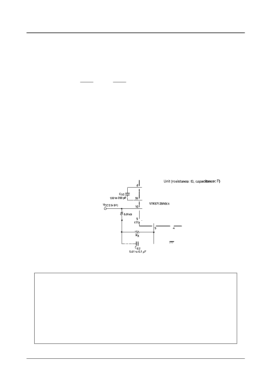
Motor hold noise countermeasures
The STK6712BMK4 executes constant current chopping outside the audible range. During motor hold the current hold
is outside the range of audible frequencies, but for motors of sizes 30 to 40 mm square (when seen from the shaft
direction) with inductance of about 15 mH, there are cases where the output noise is converted to low-frequency noise.
In this case, addition of the following components will essentially eliminate such audible noise.
Fig. 10 Motor Hold Noise Countermeasure
fclock
2
fclock
2
This catalog provides information as of October, 1995. Specifications and information herein are subject to
change without notice.
s
No products described or contained herein are intended for use in surgical implants, life-support systems, aerospace
equipment, nuclear power control systems, vehicles, disaster/crime-prevention equipment and the like, the failure of
which may directly or indirectly cause injury, death or property loss.
s
Anyone purchasing any products described or contained herein for an above-mentioned use shall:
Accept full responsibility and indemnify and defend SANYO ELECTRIC CO., LTD., its affiliates, subsidiaries and
distributors and all their officers and employees, jointly and severally, against any and all claims and litigation and all
damages, cost and expenses associated with such use:
Not impose any responsibility for any fault or negligence which may be cited in any such claim or litigation on
SANYO ELECTRIC CO., LTD., its affiliates, subsidiaries and distributors or any of their officers and employees
jointly or severally.
s
Information (including circuit diagrams and circuit parameters) herein is for example only; it is not guaranteed for
volume production. SANYO believes information herein is accurate and reliable, but no guarantees are made or implied
regarding its use or any infringements of intellectual property rights or other rights of third parties.